Sony Dej011 Service Manual
Here you can view all the pages of manual Sony Dej011 Service Manual. The Sony manuals for Portable CD Player are available online for free. You can easily download all the documents as PDF.
Page 1
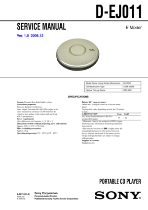
PORTABLE CD PLAYER
E Model
SPECIFICATIONS
D-EJ011
Ver. 1.0  2006.12
Model Name Using Similar Mechanism D-EJ010
CD Mechanism Type CDM-3525A
Optical Pick-up Name DAX-25E
9-887-511-012006L02-1
© 2006.12
Sony Corporation
Pe rsonal Audio Division
Published by Sony Techno Create Corporation
SERVICE MANUAL
System:  Compact disc digital audio system
Laser diode properties
Emission duration: Continuous
Laser output: Less than 44.6  µW (This output is the
value measured at a distance of 200 mm from the
objective...
Page 2
2
D-EJ011
Notes on chip component replacement• Never reuse a disconnected chip component.
• Notice that the minus side of a tantalum capacitor may be
damaged by heat.
Flexible Circuit Board Repairing • Keep the temperature of the soldering iron around 270 ˚C
during repairing.
• Do not touch the soldering iron on the same conductor of the
circuit board (within 3 times).
• Be careful not to apply force on the conductor when soldering
or unsoldering.
CAUTION
Use of controls or adjustments or performance of...
Page 3
3
D-EJ011
SECTION 1
SERVICING NOTES
NOTES  ON  HANDLING  THE  OPTICAL  PICK-UP
BLOCK  OR  BASE  UNIT
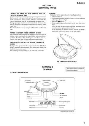
The laser diode in the optical pick-up block may suffer electrostatic
break-down because of the potential difference generated by the
charged electrostatic load, etc. on clothing and the human body.
During repair, pay attention to electrostatic break-down and also
use the procedure in the printed matter which is included in the
repair parts.
The flexible board is easily damaged and should be handled with...
Page 4
4
D-EJ011SECTION 3
DISASSEMBLY
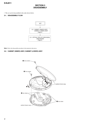
• This set can be disassembled in the order shown below.
3-1. DISASSEMBLY FLOW
3-2. CABINET (INNER) ASSY, CABINET (LOWER) ASSY
Note: Follow the disassembly procedure in the numerical order given.
3-2. CABINET (INNER) ASSY,
        CABINET (LOWER) ASSY            (Page 4)
3-3. OPTICAL PICK-UP (CDM-3525A),             MAIN BOARD
                         (Page 5) SET
4 two screws
cabinet (inner) assy
cabinet (lower) assy
3 five screws
1
2
5 two claws
6 two claws
Page 5
5
D-EJ011
3-3.OPTICAL PICK-UP (CDM-3525A), MAIN BOARD
MAIN Board (side A) To / F
rom
Optical devic
eCDM-3525A
BLK
RED
ORGGRY
4 MAIN board
cabinet (lower) assy
3 optical pick-up CDM-3525A
1 CN501
2 Unsolder four lead wires
Page 6
6
D-EJ011SECTION 4
ELECTRICAL ADJUSTMENTS
The CD section adjustments are done automatically in this set.
Adjusting Procedure: 1. Perform check in the order given.
2. Use YEDS-18 disc (Part No: 3-702-101-01) unless otherwise indicated.
3. Power supply voltage requirement :DC4.5 V in DC IN jack.    (J401)
VOLUME button : Minimum
HOLD switch :OFF
Focus bias Check
Condition:
• Hold the set in horizontal state.
Connection: Procedure:
1. Make a solder bridge to short SL801 (OPEN) on the MAIN board side B.
2....
Page 7
7
7
D-EJ011
D-EJ011
Note on Printed Wiring Boards.
• X : parts extracted from the component side.
• Y : parts extracted from the conductor side.
• a: Through hole.
• f: internal component
•
: Pattern from the side which enables seeing.
(The other layers patterns are not indicated.)
• Note for Printed Wiring Boards and Schematic Diagrams
Note on Schematic Diagrams.
•All capacitors are in  µF unless otherwise noted.  (p: pF)
50 WV or less are not indicated except for electrolytics
and tantalums.
• All...
Page 8
8
8
D-EJ011
D-EJ011
5-1. BLOCK DIAGRAM
: CD PLAY
• Signal Path
3
8079
3
5
65
1
7722
174
7
8
15161819
6463
51
6667
242350534947483962
272625242322
3
576
9
18
DRIVER
DRIVER
DRIVER
17
19
20
23
22
11
DIGITALFILTERSERVO
SIGNAL GEN.
RF
SIGNAL GEN.
OP IC
DIGITAL SERVO
SIGNAL GEN.
PD
LD
FDOUT
TDOUT
SDOUT
CLVOUT
TRK
FOCUS
20CLK88
CLK
TRK
SLED
CLV
XO
XI
SUBSYQ
MCK
DIN/DOUT
R/W
RESETX
BUSY
CLOCKOSC
DAC
31
36
21
35
SWITCHING
Q404
SWITCHINGQ403
171615
47-62
19-24,27-322,3,5,6,8,9,11,12,39,
40,42,43,45,46,48,49
43-32...
Page 9
9
9
D-EJ011
D-EJ011 5-2. PRINTED WIRING BOARD  – MAIN BOARD (SIDE A) –
 :Uses unleaded solder.
•
Semiconductor
Location
Ref. No.Location
D401 E-6
D403 D-6
D803 D-5
IC301 A-2
IC601 B-4
IC802 E-4
Q401 D-6
Q402 E-6
Q403 E-7
IC301
IC601
14
85
120 40
60
21
41
61
80
1
4
8
5
E
E
+– –+
(SLED)
M
(SPINDLE)
M
OPTICAL DEVICE (CDM-3525A) (1/2)
GRY
ORG BLK
RED
C210
R201 R205
R206 R106
R104R204
R620
R601R608 C613
C614 C615
R615 R609
R610 C609 C611C604
R606
R103
R203R616
R105
R304
R619 C108
C102
C618
R607
C605
C626...
Page 10
10
10
D-EJ011
D-EJ011
5-3.
PRINTED WIRING BOARD  – MAIN BOARD (SIDE B)  –
 :Uses unleaded solder.
• Semiconductor
Location
Ref. No.Location
D404 E-1
IC401 D-3
IC602 B-6
IC801 E-4
Q404 E-2
Q601 C-5
Q602 A-5
1
20
21 40
1 20
60
80 40
21
61
41
1
22
BP VL
1
25
26 50
DC  IN  4.5V
J401
S803.
S802 >
S807
x
S801u
LCD801LIQUID CRYSTAL DISPLAY
S812HOLD.
1 2 15
16
OPTICAL DEVICE
(CDM-3525A) (2/2)
X601
S811
(OPEN)
SL801
(OPEN)
i
J301
S804
VOL– S808
SOUND/
AVLS
S805
VOL+ S809
P MODE/
DRY BATTERY
SIZE AA
(IEC...


